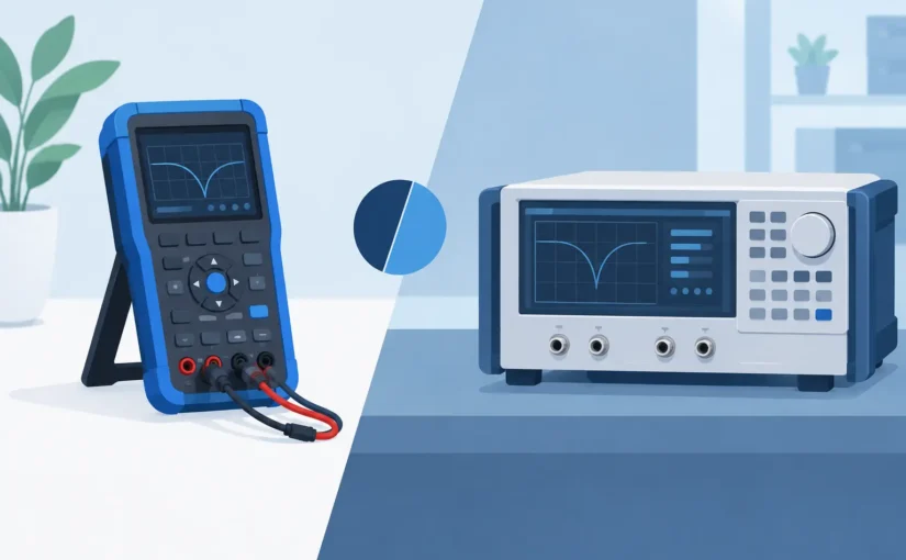
How to Identify Unmarked SMD Parts Accurately

A mixed tray of 0402 and 0603 devices is not an inventory system. Once reel labels, assembly drawings, or board documentation are missing, a visually identical group of chip resistors, MLCCs, ferrite beads, and inductors can quickly become a source of rework, scrap, or latent field failures. To identify unmarked SMD parts reliably, treat the task as a controlled measurement process rather than a visual sorting exercise.

The objective is not merely to obtain a number on a meter. It is to establish component type, nominal value, tolerance band where possible, and whether the part is suitable for its intended circuit position. That requires the right test conditions, an understanding of parasitics, and a clear boundary between what can be measured on a loose part and what must be inferred from the circuit.

Why unmarked SMD components are difficult to identify

Most small passive components carry no readable value code. On parts below 0805, markings are uncommon; on 0402 and 0201 packages, they are effectively absent. Package dimensions may narrow the possibilities, but they do not identify electrical value. A 0603 10 kOhm resistor, 100 nH inductor, 100 nF MLCC, and ferrite bead may look nearly identical from above.

Construction also affects measurements. Multilayer ceramic capacitors can lose capacitance under DC bias. Inductors and ferrite beads are frequency-dependent. Low-value resistors can be dominated by probe and contact resistance. A component measured at the wrong frequency or with unstable contact may appear to be a different part entirely.

There is a second complication: board-level measurements include the circuit connected to the component. Parallel paths lower an apparent resistance, neighboring capacitors increase an apparent capacitance, and semiconductor junctions can alter the reading as test polarity changes. A fast reading is useful for screening, but it is not automatically a valid component identification.

Start with physical and circuit evidence

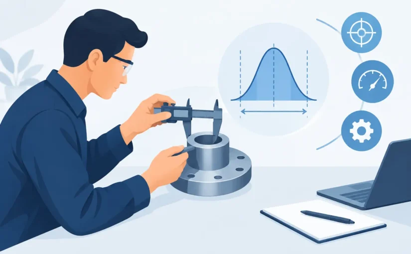
Before connecting a meter, document what is known. Measure the body length and width with a caliper or compare it against a verified package reference. Record the pad spacing, terminal finish, component color, and any top-side marking. Dark gray or black molded parts often suggest an inductor, bead, or tantalum capacitor, while the familiar beige body of an MLCC is a useful clue, not proof.

Then examine location and circuit function. A small device placed in series with a supply rail is more likely to be a bead, inductor, current-sense resistor, or jumper than a decoupling capacitor. A part connected from a power plane to ground is commonly a capacitor. Repeated footprints around an IC can reveal a decoupling network, while matched pairs close to differential lines may be terminations or common-mode filtering components.

Board reference designators are particularly valuable. R, C, L, FB, D, and Q prefixes do not guarantee that a previous repair was correct, but they establish a strong starting hypothesis. If an intact sister board is available, compare both placement and measured values. This is often more dependable than attempting to identify a part from package appearance alone.

Measure loose components first

A removed component provides the cleanest answer. Test it after it has cooled from hot-air removal and after any flux residue has been cleaned from the terminals. Residue and moisture can matter when evaluating high resistance, low capacitance, or leakage-sensitive parts.

A practical identification sequence has four stages:

  • Verify contact quality and compensate for probe resistance, fixture effects, and open/short offsets.
  • Use automatic component recognition to establish whether the device behaves primarily as R, L, or C.
  • Select a test frequency and range appropriate to the expected value, then record the primary value and dissipation factor, ESR, or quality factor.
  • Repeat the measurement after rotating the part or re-seating the contacts to confirm that the result is stable.

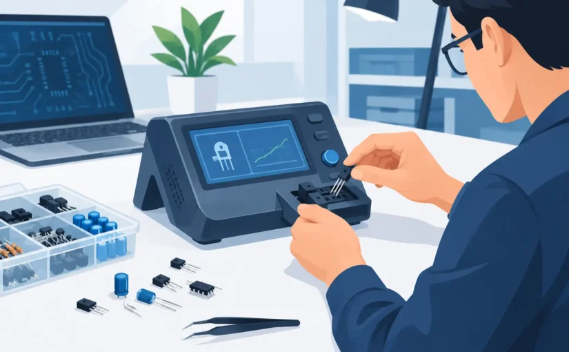
Direct-contact tweezer instruments are especially effective for this work because they avoid loose leads and allow the component to be gripped at its terminations. Smart Tweezers® instruments, for example, combine automatic R, L, and C identification with controlled test frequencies and direct-contact measurement for small chip components. For production or laboratory use, repeatability matters as much as speed: a value that shifts every time the probes touch the device is a contact or test-condition problem until proven otherwise.

Identifying chip resistors

For a resistor, begin with a low-resistance-aware measurement method. Standard two-wire probing can add enough lead and contact resistance to distort readings below a few ohms. Kelvin measurement is preferred for current-sense resistors, jumpers, and other low-ohm devices because it separates force and sense paths.

A stable 9.96 kOhm reading strongly supports a 10 kOhm nominal resistor, but it does not establish tolerance without a specification or comparison sample. For high-value resistors, allow the reading to settle. Surface contamination and finger contact can influence megohm-range results.

If a supposed resistor presents substantial reactance, check the test frequency and inspect its circuit role. It may be an inductor, ferrite bead, capacitor, or a resistor network rather than a single chip resistor.

Identifying capacitors

Capacitor measurement requires more caution than a simple capacitance number suggests. MLCCs have broad package overlap, and the value printed by a meter depends on test frequency, AC stimulus, DC bias conditions, temperature, and the capacitor dielectric. A nominal 1 uF X5R capacitor can measure materially below its marked value when biased in service.

For loose parts, measure at a frequency relevant to the expected application and compare against known-good components of the same physical size and likely dielectric family. Very low capacitance values require a clean fixture, short connections, and open compensation. At the sub-picofarad level, stray capacitance from probes, hands, solder residue, and nearby metal can exceed the component under test.

ESR and dissipation factor provide useful secondary evidence. An unexpectedly high loss reading can indicate a damaged capacitor, a poor contact, or a part that is not a capacitor at all. Do not reject an MLCC solely because its measured capacitance differs from a schematic value taken under different bias and frequency conditions.

Identifying inductors and ferrite beads

An inductor’s apparent inductance is frequency-dependent, and a ferrite bead does not behave like an ideal inductor across its working band. A bead may show a small inductance value at low frequency while its intended function is high-frequency impedance and noise suppression. That makes board position and part geometry critical evidence.

For low-value inductors, probe inductance and contact geometry become major error sources. Use short, compensated connections or direct terminal contact, and select an instrument capable of resolving low nanohenry values. Compare the measured inductance and series resistance with known-good devices when available. DC resistance is often helpful for separating a power inductor from a bead, but it cannot identify either part by itself.

Know when in-circuit testing is enough

In-circuit testing is excellent for triage. It can identify a shorted decoupling capacitor, an open series resistor, or a missing inductive path without removing parts. It is less reliable for determining the exact nominal value of a component connected to multiple parallel or active paths.

Use an in-circuit value as a screening result when the surrounding network is understood and the measurement agrees with a known-good board. Remove one terminal, or remove the component completely, when the result affects a repair disposition, incoming inspection decision, or root-cause report. Lifting one end often isolates the component with less risk than full removal, particularly for small passive parts on multilayer boards.

Do not force an RLC classification onto an unmarked diode, transistor, TVS device, or IC. These devices need polarity-aware diode testing, transistor checks, or analog signature analysis. A semiconductor can appear resistive or capacitive to an LCR meter at one stimulus level while behaving very differently under operating conditions.

Build a repeatable identification record

Once a component is identified, preserve the result. Record package size, measured value, test frequency, secondary parameter, instrument model, compensation state, and whether the part was measured loose or in circuit. Add a board location and photo when the work supports repair, quality, or failure analysis.

This record turns a one-time measurement into usable engineering data. It also exposes questionable assumptions. If ten supposedly identical capacitors produce two distinct value clusters, the tray may contain mixed stock. If a value changes only when measured on the board, the circuit is influencing the reading rather than the component itself.

The most useful outcome is not a label placed on one mystery part. It is a measurement method your team can repeat with the same controlled contact, test conditions, and confidence when the next unmarked SMD device reaches the bench.

LCR Meter Selection for Precision SMD Testing

A 0402 capacitor that reads correctly at 1 kHz can still be the wrong part for a 100 kHz switching circuit. A low-value inductor measured through long clip leads can appear to have more inductance than the part itself. These are not minor inconveniences. They are the measurement conditions that determine whether an LCR meter supports a defensible engineering decision or merely produces a number.

For component evaluation, incoming inspection, repair, and failure analysis, the useful question is not simply whether an instrument measures inductance, capacitance, and resistance. It is whether it can measure the component at a relevant test frequency, with controlled parasitics, sufficient resolution, and a measurement model that matches the device under test.

What an LCR Meter Actually Measures

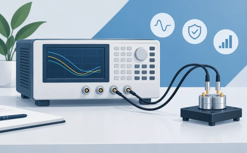
An LCR meter applies an AC test signal to a component and evaluates the resulting voltage-current relationship. From magnitude and phase, it calculates a primary parameter – inductance (L), capacitance (C), or resistance (R) – and a secondary parameter such as dissipation factor (D), quality factor (Q), equivalent series resistance (ESR), phase angle, or impedance magnitude.

This matters because real components are not ideal. A capacitor includes dielectric loss and series resistance. An inductor has winding resistance, core loss, and self-capacitance. A resistor can become inductive at frequencies where its package geometry and construction are no longer negligible. The displayed value is therefore a representation of the part under specific electrical conditions, not a permanent label printed by the instrument.

Most instruments can automatically identify a component as a resistor, capacitor, or inductor. Automatic identification is valuable for fast sorting and mixed-component work, but it should not replace engineering judgment. Near resonance, or with lossy, damaged, or complex networks, more than one model may appear plausible. Review the primary reading, secondary reading, test frequency, and measurement mode before accepting a result.

LCR Meter Specifications That Drive Useful Results

Basic accuracy is often the first specification compared, and it should be. A 0.1% basic accuracy specification offers a substantially stronger basis for component verification than a general-purpose handheld reading with broad uncertainty. Yet accuracy alone does not define measurement capability.

Test frequency is equally consequential. Capacitance, inductance, ESR, Q, and D can vary significantly across frequency. A meter operating only at low frequencies may be adequate for broad inventory checks, while it may not reveal behavior relevant to high-frequency power stages, RF-adjacent circuitry, or small ceramic capacitors. For demanding SMD evaluation, test frequencies extending to 250 kHz provide a more useful window into component behavior than single-frequency testing.

Resolution and range determine whether the instrument can see the values that matter. Sub-1 pF capacitance capability is not simply a headline specification when diagnosing a PCB pad, a small capacitor, or fixture-induced stray capacitance. Likewise, sub-10 nH inductance measurement can be decisive when evaluating low-inductance coils, traces, jumpers, and high-current interconnects. At these levels, however, the fixture and measurement technique become inseparable from the meter itself.

A practical LCR meter selection should examine these specifications together:

  • Basic accuracy over the intended measurement range, not only a best-case figure.
  • Available test frequencies and whether they match the component’s operating environment.
  • Lowest and highest supported capacitance, inductance, resistance, and ESR values.
  • Series and parallel equivalent-circuit modes, plus secondary parameter reporting.
  • Open, short, and load calibration capability for the selected fixture.
  • Data recording, remote control, or Bluetooth connectivity when traceable records are required.

The right balance depends on the task. Production screening may prioritize speed and repeatability. Failure analysis may prioritize frequency control, low-value resolution, and complete documentation. Field repair may require direct component contact without moving a board to a bench fixture.

Why Fixturing Can Matter More Than the Display

At ordinary component values, clip leads may be acceptable. At picofarad and nanohenry levels, they are a source of measurement error. Lead length adds inductance. Insulation, probe spacing, and nearby conductors add capacitance. Contact resistance can distort ESR and low-resistance readings. The meter cannot distinguish a component from unwanted impedance introduced by the test setup unless that setup is controlled and calibrated.

For loose SMD components, direct-contact tweezers reduce loop area and eliminate the repeated handling associated with clips or socket fixtures. The workflow benefit is obvious during sorting or repair, but the metrology benefit is more significant: shorter current paths and stable contact geometry help reduce parasitic effects. This is especially useful for 0201, 0402, and 0603 components that are difficult to hold and easy to misidentify.

For cabled measurements, Kelvin connections separate the current-carrying and voltage-sensing paths. This minimizes errors caused by lead and contact resistance, particularly when measuring low resistance, ESR, or low-impedance inductors. A four-wire connection is not automatically required for every part, but it becomes increasingly valuable as the impedance under test approaches the resistance of the probes and contacts.

Calibration must follow the fixture. An open correction characterizes residual stray capacitance. A short correction accounts for lead inductance and residual resistance. A load verification checks performance against a known standard. If probes, cables, or connectors change, repeat the appropriate compensation. Calibration performed with one setup does not transfer perfectly to another.

Selecting Series or Parallel Measurement Mode

Series and parallel modes are equivalent-circuit models. They are not cosmetic display options.

A low-loss capacitor often aligns with a series model, expressed as capacitance with ESR. A high-impedance or lossy component may be better represented with a parallel model, expressed as capacitance with parallel resistance. Similarly, a low-impedance inductor often suits a series model, while a high-impedance inductor or coil may be more meaningful in parallel mode.

There is no universal setting that is correct for every component. Select the model based on the component’s impedance, loss mechanism, data-sheet convention, and intended application. When comparing an incoming part against a manufacturer specification, use the same test frequency, AC level when available, DC bias condition, and equivalent-circuit model stated in that specification. Otherwise, a disagreement may be caused by unlike conditions rather than a defective component.

Build Measurement into the Workflow

A capable handheld instrument changes what can be tested at the point of work. A technician can verify a removed component before installation, compare suspected parts at a repair station, or assess inventory without setting up a conventional bench analyzer. This reduces unnecessary rework, but speed should not become an excuse for uncontrolled testing.

Start with the component marking, bill of materials, or data sheet. Establish the expected value and tolerance, then select an appropriate frequency and model. Zero or compensate the fixture at the beginning of the session. For critical values, measure a known reference component before and after a group of tests. If readings drift, contacts are unstable, or values vary with probe pressure, investigate the setup before classifying parts as failed.

For quality systems, record the conditions with the result. A capacitance value without frequency, mode, and fixture information has limited audit value. Bluetooth-enabled logging or remote data capture can reduce transcription errors and create a usable trace from receiving inspection through corrective action. Calibration-backed instruments and reference standards support the same discipline when results must be compared across technicians, locations, or time.

When a Portable Meter Is the Better Instrument

A bench LCR analyzer remains appropriate for characterization requiring the widest frequency range, specialized biasing, automated handlers, or highly controlled laboratory fixtures. Portability is not a replacement for every bench capability.

But many electronics decisions happen where the part is, not where the bench is. Direct-contact instruments such as LCR-Reader Smart Tweezers® bring precision measurement to populated boards, incoming trays, field kits, and repair stations. For tasks centered on rapid identification, SMD verification, low-value measurement, and repeatable pass/fail assessment, the reduction in setup time can be as valuable as the specification itself.

The strongest measurement process is the one that makes correct technique practical enough to use every time. Select an instrument whose frequency range, accuracy, fixturing, compensation, and data controls match the components in front of you, then let the measurement conditions travel with every result.

Choosing a Handheld Multimeter Oscilloscope

A board powers up but resets whenever a relay closes. The DC rail looks correct on a conventional meter, yet the failure is still present. This is the point where a handheld multimeter oscilloscope earns its place: it can report the numeric supply value while exposing the transient, ripple burst, or switching noise that the number hides.

For field technicians, production engineers, and repair specialists, the appeal is obvious. One portable instrument can verify voltage, resistance, continuity, frequency, and current while providing a time-domain view of a signal. The limitation is equally important: a combined instrument is not automatically a replacement for a full bench oscilloscope, a precision handheld DMM, or a dedicated LCR meter. Selecting the right unit requires matching measurement architecture to the signals, safety category, accuracy requirements, and documentation demands of the job.

What a Handheld Multimeter Oscilloscope Actually Combines

A handheld multimeter oscilloscope, often called a scope meter or oscilloscope multimeter, combines two distinct measurement functions. The digital multimeter section measures values such as DC and AC voltage, current, resistance, capacitance, frequency, duty cycle, and diode drop. The oscilloscope section captures voltage as it changes over time, allowing the user to inspect waveform shape, timing, noise, overshoot, dropout events, and modulation.

These functions answer different questions. A DMM answers, “What is the measured value?” An oscilloscope answers, “What happened during the measurement interval?” A 24 V supply that reads 24.03 V can still contain a 300 mV switching ripple, a 2 ms sag under load, or an intermittent startup spike. Each condition may matter in a control system, automotive module, power converter, or sensitive analog front end.

The best combined instruments keep the two workflows accessible rather than forcing a technician to navigate complex menus for basic checks. In practical troubleshooting, continuity checks and DC rail verification happen constantly. Waveform capture is needed when a circuit behavior is dynamic, intermittent, or load-dependent.

Bandwidth and Sample Rate Define What You Can See

Bandwidth is one of the first oscilloscope specifications to evaluate. It defines the approximate frequency range over which the instrument can display a signal with acceptable amplitude response. For low-frequency control, sensor, audio, relay, and many power-supply tasks, modest bandwidth may be sufficient. For clock signals, fast digital interfaces, switch-mode power edges, and RF-adjacent circuits, it may not be.

A common rule is to select bandwidth at least five times higher than the highest fundamental frequency of interest. That is a starting point, not a complete criterion. Fast square-wave edges contain high-frequency harmonics. An instrument with inadequate bandwidth can make a fast edge appear slow and can conceal ringing or overshoot that is relevant to EMI, component stress, and logic reliability.

Sample rate must be considered with bandwidth. Real-time sample rate determines how frequently the waveform is digitized. If it is too low, the display can miss narrow pulses or create aliasing, where a high-frequency signal appears as a false lower-frequency pattern. For repetitive waveforms, equivalent-time sampling can extend apparent performance, but it is not a substitute for adequate real-time sampling when diagnosing an intermittent event.

Memory depth matters after an event is captured. A short record can show a clean, detailed switching edge but provide little context before and after it. A deeper acquisition can preserve startup behavior, communication bursts, load transitions, or a long sequence of power events. The trade-off is often update rate, file size, and interface complexity. For field diagnosis, event capture and waveform recall can be more valuable than laboratory-grade record length.

Triggering Separates Useful Captures From Random Screens

Trigger capability is where a scope meter moves from a visual indicator to a diagnostic instrument. Edge triggering is essential, but pulse-width, timeout, slope, and single-shot triggering can be decisive when failures are infrequent.

Consider an industrial 24 V rail that drops for a fraction of a second only when a solenoid is energized. A stable trigger level, single acquisition mode, and saved waveform can establish whether the issue is a supply limitation, a wiring fault, or switching interference. Without triggering, the technician may only see a moving trace and an unresolved complaint.

DMM Specifications Still Matter

The oscilloscope feature tends to draw attention, but the multimeter section determines whether the instrument can support daily verification work. Look beyond the number of functions. Basic DC voltage accuracy, resolution, input impedance, AC measurement bandwidth, current ranges, burden voltage, and update rate all affect the result.

True-RMS AC measurement is relevant when waveforms are not sinusoidal. Variable-frequency drives, switching supplies, dimmers, and distorted mains environments can produce readings that a basic average-responding meter does not represent correctly. True RMS alone is not a guarantee of performance, however. The meter must also specify the crest factor and AC bandwidth over which that accuracy applies.

Current measurement deserves special caution. Inserting a meter in series can interrupt operation and add burden voltage, changing the behavior of a low-voltage circuit. For higher current work, a compatible current clamp is often safer and less intrusive. Confirm whether the instrument supports clamp scaling and whether it can display current and voltage together for power troubleshooting.

For precision component work, a combined scope meter is not necessarily the correct instrument. Capacitance and resistance readings made through ordinary test leads can be affected by lead resistance, contact quality, fixture parasitics, and test conditions. Very small capacitance, inductance, and ESR values require an instrument designed for those ranges and a measurement method that controls parasitic effects. Direct-contact tools such as LCR-Reader instruments address a different, complementary task: rapid, calibrated characterization of components rather than waveform analysis of an operating circuit.

Safety Rating Is a System Specification

A handheld instrument used near energized equipment must be evaluated as a complete measurement system. The label on the meter is only one element. Probe ratings, leads, adapters, current clamps, fuses, connector shrouds, and working practices must be suitable for the installation category and voltage involved.

CAT ratings describe the transient environment an instrument is intended to withstand, not simply its maximum steady-state voltage. A measurement point inside a low-energy electronic assembly is not equivalent to a building distribution panel or an outdoor service entrance. Technicians should select the applicable category based on the measurement location, then verify that every accessory used in the test path meets or exceeds that requirement.

Oscilloscope inputs introduce another issue: channel reference and isolation. Many bench oscilloscopes have input grounds tied together and connected to protective earth. Connecting a grounded probe to the wrong point in a mains-referenced circuit can create a destructive short circuit. A battery-powered handheld unit may offer isolated channels, but isolation architecture varies. Read the channel-to-channel and channel-to-ground specifications before probing inverter outputs, motor drives, high-side gate circuits, or floating power stages.

Evaluate the Workflow, Not Just the Specification Table

A technically capable handheld instrument can still slow work if it is difficult to operate with gloves, unreadable in bright light, or unable to preserve evidence. Display size, contrast, probe storage, input labeling, battery runtime, charging method, and physical durability matter on a production floor or at a service site.

Data capture is increasingly part of the measurement requirement. Saved screenshots are useful for repair records, while waveform files and logged meter readings support trend analysis, failure reports, and quality documentation. Verify file formats, timestamp behavior, internal storage capacity, export method, and whether software is required to view the captured data. Bluetooth or USB connectivity can reduce manual transcription, but only if the workflow fits controlled manufacturing or laboratory procedures.

Calibration should also be treated as an operational requirement. If measurements support acceptance testing, maintenance records, or customer reports, establish the calibration interval, available certificate options, adjustment process, and traceability requirements before purchase. A high specification is useful only when measurement performance can be maintained and documented over the instrument’s service life.

Match the Instrument to the Fault

For general electronic service, prioritize a responsive DMM, clear display, safe input protection, basic triggering, and enough bandwidth to inspect rails, clocks, PWM, and sensor outputs. For power electronics and industrial maintenance, isolation, transient safety, current-clamp support, long recording capability, and event triggering may be more valuable than extreme bandwidth.

For embedded systems, evaluate digital pulse capture, serial-bus decoding if needed, timing resolution, and the ability to compare two related signals. One channel may show that a clock exists; two synchronized channels can show whether reset releases at the correct time relative to power-good or enable. The difference is often the difference between observation and diagnosis.

A handheld multimeter oscilloscope delivers its strongest value when it reduces the number of trips between the fault, the bench, and the tool cabinet. Choose one that captures the behavior your present meter cannot explain, protects the user at the actual measurement point, and produces results that another engineer can verify. That is the standard worth carrying into the field.

How to Choose an SMD Component Tester for PCB Work

A 0402 capacitor that looks perfect under magnification can still be the reason a production board fails functional test. The practical value of an SMD component tester is not simply that it displays capacitance, resistance, or inductance. It is that it provides a fast, repeatable measurement at the component itself, where a technician or engineer can separate a suspect part from fixture error, assembly damage, or an incorrect reel before time is lost.

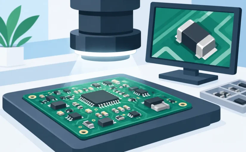
For surface-mount work, measurement technique matters as much as the displayed digits. Small components have small values, tight tolerances, and lead-free terminations that are easy to contact poorly. A useful tester must control the variables that distort low-value measurements: probe contact resistance, stray capacitance, lead inductance, test frequency, and the influence of surrounding circuitry.

What an SMD Component Tester Must Measure

At minimum, an SMD tester should identify and measure resistors, capacitors, and inductors. Automatic component identification is valuable when sorting mixed inventory, verifying unknown parts on a bench, or inspecting boards with incomplete documentation. It reduces setup time, but it should not replace engineering judgment. A device may report a nominal capacitance while the parameter that explains the failure is ESR, dissipation factor, or impedance at the operating frequency.

For capacitors, look beyond a broad capacitance range. A meter intended for serious PCB work should resolve very low capacitance values while maintaining a controlled measurement method. At the low end, a fraction of a picofarad from fingers, probe spacing, a contaminated fixture, or nearby conductors can exceed the value being measured. At the high end, the instrument must handle larger capacitors without making the workflow slow or forcing repeated range changes.

Inductance places a different demand on the tester. Very small inductors and ferrite beads can have values close to the inductance contributed by ordinary test leads. Direct-contact tweezer measurement minimizes the loop area that creates this error. Sub-10 nH capability is meaningful only when the instrument, probes, calibration procedure, and operator technique all support it.

Resistance measurements also benefit from direct contact. For low-ohm parts, probe and contact resistance can become a significant part of the reading. Where low resistance is critical, Kelvin-style measurement methods or connectors that separate current drive from voltage sensing are preferable. A two-wire reading may be adequate for verifying a 10 kOhm resistor, but it is not the same test as characterizing a 20 mOhm current-sense resistor.

Test Frequency Changes the Answer

An ideal capacitor has one capacitance value. A real multilayer ceramic capacitor has capacitance, ESR, dielectric loss, DC-bias behavior, and frequency-dependent impedance. Likewise, an inductor has winding resistance, core losses, parasitic capacitance, and a self-resonant frequency. The test frequency selected by an SMD component tester therefore changes what is being evaluated.

A low test frequency may be appropriate for general component identification and bulk capacitance checks. Higher frequencies are more informative for small ceramic capacitors, RF-related inductors, ferrite beads, and components used in switching power stages. A tester with frequencies extending to 250 kHz offers a more relevant window into many modern circuit behaviors than a single low-frequency measurement.

That does not mean the highest available frequency is always the right choice. Test at a frequency that supports the decision you need to make. When receiving capacitors for a power rail, compare parts under the same frequency and test conditions used in your approved process. When diagnosing an RF matching network, the tester can identify a missing, cracked, or incorrect-value part, but a network analyzer may still be required to evaluate the circuit at its actual operating frequency.

Direct Contact Is a Measurement Advantage

Conventional probes can measure SMD components, but they introduce a basic workflow problem: one hand stabilizes the part or board, another hand manages two probes, and contact quality changes from measurement to measurement. On 0201 or 0402 components, that process is slow and can easily produce intermittent readings.

Tweezer-form instruments address this directly. Two fixed, closely spaced tips contact both terminations with a controlled geometry. The measurement path is shorter, the parasitic loop is smaller, and the operator can lift a loose component from tape, tray, or bench while reading its value. For repair work, the same geometry makes it practical to inspect a component installed on a board without searching for test points.

This is also where mechanical details become electrical details. Tip cleanliness, spring pressure, alignment, and oxidation affect repeatability. Fine tips should be kept clean and undamaged. Before measuring low capacitance or low inductance values, perform the instrument’s prescribed open and short calibration with the actual probe configuration. Calibration is not an optional ritual – it establishes a reference that removes predictable fixture effects from the result.

In-Circuit Testing Has Clear Limits

In-circuit measurement is one of the most productive uses of a portable component tester, but it is not a promise that every displayed value belongs only to the selected part. Parallel components, semiconductor junctions, IC protection structures, and power-rail capacitors can all create alternate paths.

A resistor in a simple series path may measure accurately in circuit. A capacitor across a supply rail will often read as the combined effect of every capacitor and circuit path connected to that rail. An inductor in a switching converter can be influenced by the controller, catch diode or synchronous MOSFETs, output capacitors, and the state of the unpowered circuit.

Use in-circuit readings as comparative evidence. Measure the corresponding component on a known-good board, inspect the same reference designator across multiple assemblies, or compare a suspect part with an adjacent part of the same value. If the result remains ambiguous, isolate one terminal or remove the component. A fast direct-contact reading helps determine whether that extra rework step is justified.

Specifications That Support Better Decisions

A specification sheet should be read as a measurement system, not as a list of maximum ranges. Basic accuracy matters, but accuracy alone does not describe performance at every value, frequency, and impedance. Review the stated test conditions and determine whether they resemble your application.

For professional PCB evaluation, prioritize these capabilities:

  • Broad R, L, and C ranges that cover the component families your team actually handles.
  • Resolution suitable for low-pF capacitors and low-nH inductors, not only large nominal values.
  • Multiple test frequencies, particularly when evaluating high-frequency bypassing, inductors, and ferrite components.
  • ESR, dissipation factor, quality factor, and impedance functions when component loss or frequency behavior is relevant.
  • Automatic identification that accelerates sorting without obscuring the measured parameter and test condition.
  • Calibration support with documented procedures and, where required, traceable calibration options.
  • Data recording when inspection results must be retained for quality, failure analysis, or process validation.

Bluetooth logging can be particularly useful when technicians need to document a sequence of measurements without manually transcribing values. In a quality-control environment, that reduces transcription errors and creates a more defensible record. It does not replace a defined inspection plan, but it makes that plan easier to execute consistently.

Build the Tester Into the Workflow

The best instrument is the one that shortens the path from a suspect part to a defensible decision. For incoming inspection, establish known-good measurements for critical components and record the frequency, test mode, and calibration state. For troubleshooting, begin with unpowered-board checks and compare against a known-good assembly before removing parts. For rework verification, measure the replacement component before installation, then confirm that the board-level result matches expectations after soldering.

Educators can use the same approach to show why a resistor is usually straightforward while a capacitor or inductor requires attention to frequency and parasitics. Manufacturing teams can use it to prevent component mix-ups before reels reach placement equipment. Repair specialists can use it to avoid replacing several expensive ICs when the fault is a cracked ceramic capacitor or an open ferrite bead.

Instruments such as Smart Tweezers® are designed around this direct-contact workflow: portable measurement, automatic identification, and the precision needed to evaluate small surface-mount parts without building a bench setup around every question.

The Practical Standard for Selection

Choose an SMD component tester based on the smallest values, tightest tolerances, and most demanding decisions in your work – not on the largest range printed on the front panel. A general-purpose meter may be sufficient for occasional loose-component checks. A production, laboratory, avionics, or advanced repair environment needs controlled contact geometry, appropriate test frequencies, low-value resolution, repeatable calibration, and measurement data that can stand behind a pass, fail, or rework decision.

When a tiny component determines whether a board ships, the useful question is not whether the tester can produce a number. It is whether the number was measured under conditions that let your team act on it with confidence.

Analog Signature Analysis for PCB Repair

A board can pass visual inspection, show no obvious thermal damage, and still contain a failed semiconductor junction, a leaky capacitor, or a shorted IC input. Analog signature analysis for PCB repair gives technicians a fast way to locate those faults without powering the board or removing every suspect component. Instead of asking only, “What is this component’s value?”, it asks, “How does this circuit node behave electrically compared with a known-good node?”

That distinction matters on dense assemblies where components are connected in parallel, schematics are incomplete, and applying power may place an expensive board at further risk. Used correctly, analog signature analysis is a comparative diagnostic method that narrows the fault area quickly. It does not replace precision LCR, ESR, voltage, or waveform measurements. It tells the technician where those more specific measurements will produce the highest value.

What Analog Signature Analysis Measures

Analog signature analysis, often called ASA or VI signature analysis, applies a controlled AC stimulus to an unpowered test point and observes the resulting current-versus-voltage relationship. The instrument displays that relationship as a trace. A resistor, capacitor, diode, transistor junction, and integrated-circuit input each produce a characteristic response because each presents a different impedance and nonlinear behavior.

A purely resistive path typically produces a straight diagonal line. The slope changes with resistance: lower resistance produces a flatter trace, while higher resistance produces a steeper trace. Capacitive and inductive behavior introduces an elliptical pattern because current and voltage are phase shifted. Semiconductor junctions produce curved or asymmetric signatures as conduction begins in one direction.

The useful result is not a catalog of ideal shapes. Real PCBs contain component tolerances, parallel paths, protection devices, and circuit loading. The diagnostic value comes from comparison. When the same node on a good board produces one signature and the suspect board produces a distinctly different one, the difference is evidence of a fault or a meaningful circuit-state change.

Why Analog Signature Analysis for PCB Repair Works

Most board-level failures change impedance before they become easy to identify with a conventional continuity test. A shorted ceramic capacitor may look like a low-resistance path. A degraded diode may conduct too early or differently in reverse bias. An ESD-damaged IC pin may not be fully shorted, yet its signature can differ markedly from the matching pin on a good board.

ASA is particularly effective because it is performed with the assembly unpowered. That reduces the chance of energizing a shorted supply rail, triggering intermittent firmware behavior, or damaging a sensitive load while troubleshooting. It also allows a technician to examine a circuit systematically when a board has no accessible test firmware or when its normal operating sequence is unknown.

A known-good reference is the central requirement. It may be an identical working PCB, a redundant channel on the same assembly, or a repeated circuit section. Comparing left and right audio channels, identical driver stages, multiple power phases, or replicated I/O circuits can reveal an outlier rapidly. A comparison between unlike nodes is much less meaningful.

Reading Signatures Without Overinterpreting Them

The most common mistake in signature analysis is treating every curve as a definitive component identification. On an assembled PCB, the signature is the response of the entire network connected to the probe point. A diode trace may include a resistor divider. A capacitor trace may be altered by a parallel IC input. A supply rail can show the combined behavior of dozens of decoupling capacitors and semiconductor protection structures.

For that reason, the first question is not “Which component makes this shape?” It is “Does this point match the corresponding point on the reference?” A symmetric circuit should generally show symmetric signatures when measured using the same ground reference, range, stimulus level, and probe orientation.

Probe polarity also matters. Reversing the probes reverses the display relationship and can change the apparent behavior of polarized devices and junctions. Maintain a documented probe convention throughout the inspection. If a difference is observed, repeat the measurement to rule out poor probe contact, contamination, an oxidized pad, or a shifted test position.

Stimulus level and frequency influence the result as well. Low-level testing may avoid turning on certain junctions, while a higher stimulus can reveal nonlinear conduction. Frequency changes the apparent response of capacitive and inductive paths. Consistent settings are essential when comparing boards. A signature library built with mixed settings is not a reliable repair reference.

Common Fault Patterns

A rail that produces a much flatter signature than the reference often indicates excess conductance, such as a shorted capacitor, damaged regulator, or failed IC. A signature that becomes more vertical may indicate an open connection, lifted component, broken trace, or increased resistance in the path.

An asymmetric trace where the reference is symmetric can point to a diode, transistor junction, or ESD structure that has changed behavior. A distorted ellipse in a timing or filtering network may indicate a capacitor with altered effective capacitance, excessive leakage, or an added parallel path. These patterns are starting points for investigation, not final diagnoses.

A Controlled PCB Repair Workflow

Begin with the board fully de-energized. Disconnect batteries, external supplies, and stored-energy sources. Allow large capacitors to discharge safely, then verify the rail voltage before connecting the analyzer. Analog signature work on a partially powered assembly can produce misleading results and may damage the instrument or board.

Establish a stable reference ground close to the circuit under test. Then inspect broad functional areas first: input power, primary and secondary rails, major connectors, repeated channels, and suspect IC pins. This approach prevents the technician from spending time probing every component before identifying the region where the signatures diverge.

When a mismatch appears, move inward. Compare adjacent nodes, both sides of series resistors or ferrite beads, nearby decoupling capacitors, and corresponding pins on duplicated circuits. The goal is to determine whether the abnormal response follows a rail, stops at an isolation component, or is localized to one device connection.

Document the measurements with board revision, test point, reference location, instrument settings, and probe orientation. In production repair and quality environments, this turns a one-time observation into repeatable evidence. Bluetooth-enabled recording instruments can further support trace capture and comparison when documentation requirements extend beyond a technician’s bench notes.

Where Precision LCR and ESR Measurement Take Over

ASA is excellent for locating an anomaly, but it cannot always separate a failed part from the network around it. Once the suspect area is isolated, direct component measurement provides the confirmation needed for a reliable repair decision.

For example, a distorted signature around a switching regulator output may identify the output capacitor bank as the likely region. An ESR measurement can then identify a capacitor whose loss is excessive under the relevant test conditions. A precision LCR measurement can verify capacitance, inductance, resistance, dissipation factor, or quality factor where the board topology permits. If parallel paths mask the result, lifting one terminal may still be necessary.

This is where direct-contact tweezer measurement is valuable. Small SMD components can be measured at the pads with controlled contact and minimal lead length, reducing errors caused by test leads and handling. Smart Tweezers® instruments are designed for this workflow, combining automatic component identification with precision measurements for values that are difficult to evaluate using a general-purpose meter alone.

The trade-off is clear: in-circuit measurements are fast but affected by surrounding circuitry; out-of-circuit measurements are more definitive but require time and may risk pad damage during removal. The best repair process uses the least invasive test that can support a confident decision.

Limits That Protect Good Diagnostics

Analog signature analysis is not a substitute for powered functional testing. It will not verify firmware execution, clock integrity under operation, switching-node waveforms, communication timing, or load regulation. A board can match a reference while still failing only under temperature, current, vibration, or software-controlled conditions.

It is also less decisive when no valid reference exists. In that case, schematics, expected component behavior, localized LCR and diode testing, and voltage-resistance comparisons become more important. Building a signature archive from known-good production boards is therefore a practical investment for repair departments handling recurring assemblies.

The strongest technicians do not use one instrument mode as a verdict. They use analog signatures to find the electrical difference, precision measurements to identify the failed element, and controlled power-up testing to prove that the repair restored the required circuit behavior. That sequence protects the board, shortens fault isolation, and creates repair evidence that can be repeated on the next difficult assembly.

Kelvin Probes for Low Resistance Measurements

A 3 mΩ solder joint can look identical to a sound joint on a production board. A standard two-wire resistance check may report a value dominated by probe leads, oxide at the tips, and inconsistent hand pressure instead of the joint itself. Kelvin probes for low resistance address that problem by separating the current path from the voltage-sensing path, allowing the instrument to measure the voltage drop at the device under test rather than across the entire test setup.

That distinction becomes decisive when verifying shunts, connectors, battery tabs, cable terminations, relay contacts, copper traces, and soldered power paths. At milliohm and sub-ohm levels, the measurement method is not an accessory choice. It is part of the specification.

Why low-resistance measurements fail with two wires

Every two-wire resistance measurement includes resistance that is not part of the component or connection under test. The meter forces current through two leads and measures voltage through those same leads. The displayed result therefore includes lead resistance, probe-tip contact resistance, fixture resistance, and the resistance of the DUT.

For a 100 Ω resistor, a few hundred milliohms of added resistance is insignificant. For a 5 mΩ current shunt or a 20 mΩ connector interface, it can overwhelm the result. Temperature makes the problem less predictable. Copper leads change resistance with temperature, while probe contact resistance changes with pressure, surface finish, contamination, and oxidation.

Zeroing a two-wire meter can remove a fixed lead contribution at one moment. It cannot reliably remove a contact resistance that changes each time a technician touches a new test point. This is why a measurement can appear stable on a clean calibration short yet vary on an actual assembly.

How Kelvin probes for low resistance work

A Kelvin connection uses four conductors, even when they are integrated into a compact probe or tweezer-style fixture. One pair, called the force pair, applies a known test current through the DUT. A separate pair, called the sense pair, measures voltage directly at or very near the DUT terminals.

The sense input draws extremely little current. Because nearly no current flows through the sense leads, their voltage drop is negligible. The instrument calculates resistance from the measured voltage and known current:

`R = V / I`

The force lead and contact drops occur outside the sensed measurement points. As a result, their influence is largely excluded from the displayed resistance. The word “largely” matters. Four-wire methods sharply reduce lead-related error, but they do not make poor probing, thermal effects, or unsuitable test conditions disappear.

A practical Kelvin probe places both force and sense contacts at each end of the DUT. On a shunt resistor, for example, force current should enter through the outer contact points while voltage is sensed at the inner points, as close as possible to the resistor terminations. This arrangement prevents the resistance of the high-current path from being included in the sense reading.

Probe placement determines the result

The best Kelvin instrument cannot correct a probe arrangement that senses the wrong section of a conductor. This is a common source of disagreement between incoming inspection, manufacturing test, and failure analysis measurements.

Consider a crimp terminal. Measuring from the wire several centimeters away to the mating contact may be appropriate for evaluating the complete assembled path. Measuring directly across the crimp barrel evaluates the crimp interface. Measuring only the terminal body says little about either. Each setup can produce a valid number, but the number answers a different engineering question.

For PCB work, place the sense points inside the force points whenever possible. On wide copper pours or bus bars, make the measurement geometry repeatable from unit to unit. A small change in probe spacing can change the measured resistance because the test current spreads through the conductor rather than following a single ideal line.

Surface condition also matters. Nickel plating, oxidation, flux residue, conformal-coating remnants, and worn probe tips introduce instability at the contact interface. If repeated readings wander, do not assume the DUT is unstable before checking the probe contact. Inspect tip condition, use controlled contact pressure, and clean approved test locations when the process permits it.

Selecting a Kelvin probe configuration

The appropriate configuration depends on DUT geometry, expected resistance, test current, and throughput requirements. Separate Kelvin clips are flexible for cables, terminals, and larger connections. Their trade-off is slower placement and greater dependence on operator technique. Fixed fixtures improve repeatability in production but require dedicated tooling and periodic verification.

Kelvin tweezers or compact probe connectors are effective where access is limited and the component is small. They can shorten the path between instrument and DUT, reduce setup time, and support direct contact with small SMD components or board-level features. The limitation is mechanical: the contact spacing and tip geometry must match the part and pad layout.

When comparing probe options, evaluate more than the connector style. Four specifications and characteristics deserve attention:

  • Current-carrying capacity of the force contacts at the intended test current
  • Tip geometry, spacing, and material for the target pads, terminals, or conductors
  • Lead length and shielding requirements for the instrument and environment
  • Defined calibration and verification practices for the complete instrument-probe system

Higher test current increases the voltage developed across a low resistance and can improve resolution. It also increases self-heating. A 1 mΩ shunt measured at 1 A dissipates 1 mW, while the same shunt at 10 A dissipates 100 mW. Depending on the shunt construction, test duration, and thermal mass, that heating can shift the resistance during measurement. Pulsed or brief measurements may be preferable for temperature-sensitive parts.

Establishing a repeatable measurement process

Start by defining the measurement plane: the exact two locations between which resistance is to be accepted or rejected. Document it with a fixture drawing, board image, or work instruction. Without a defined measurement plane, a milliohm limit is not fully actionable.

Next, verify the system with a known low-resistance standard or a controlled short appropriate to the instrument’s procedure. This confirms cable continuity, contact integrity, and basic system response. A zero or relative function is useful for setup, but it should not replace periodic verification against a known value when measurement decisions affect product quality.

Apply the probes consistently. The force and sense contacts must both be engaged at each terminal, without bridging adjacent pads or contacting contaminated areas. Allow the reading to settle according to the instrument’s measurement rate and filtering settings. For production work, record the test current, measurement time, range, and ambient conditions whenever they influence acceptance limits.

Repeatability should be assessed with realistic handling. A method that produces excellent results when one experienced engineer holds the probes may not survive shift-to-shift manufacturing use. If operator variation is large, use a guided fixture, spring-loaded contacts, or a mechanical stop that controls location and pressure.

Common errors that Kelvin connections do not solve

A four-wire measurement removes much of the lead resistance error, but it does not prove that the reported number represents the intended electrical behavior. Thermoelectric voltages can affect very low-level DC measurements, particularly across dissimilar metals and temperature gradients. Current reversal, offset compensation, or an AC test method may be needed when the instrument supports it.

Inductance can also distort measurements of bus bars, coils, long cables, and high-current paths, especially at elevated test frequency. The measured impedance then includes resistive and reactive components. Choose a test frequency and measurement mode that match the specification being verified, and keep force and sense routing controlled.

Parallel paths are another frequent trap. Measuring resistance in-circuit may include alternate copper routes, semiconductor junctions, capacitors, or parallel components. A very low reading may indicate an effective parallel network rather than a healthy single connection. Isolate the circuit when the diagnostic question requires the resistance of one element.

Finally, distinguish resolution from accuracy. An instrument that displays 0.001 mΩ is not automatically capable of an accurate 0.001 mΩ result in a real fixture. Meaningful low-resistance work requires suitable accuracy, stable test current, appropriate range selection, calibrated performance, and a probe system matched to the DUT.

Where portable Kelvin measurement adds value

Portable instruments change the workflow when the test point is on a board, in a field enclosure, or at an incoming-inspection station rather than on a bench fixture. Engineers can compare suspect and known-good assemblies directly, verify low-ohm components before installation, and locate resistive interconnect faults without moving hardware to a larger test system.

For component-level work, LCR-Reader instruments and compatible Kelvin accessories support direct-contact measurement where lead and contact effects would otherwise obscure small values. The operational advantage is speed, but the engineering advantage is a measurement taken at the component or connection itself, with a defined and repeatable contact geometry.

The most useful low-resistance result is not merely the smallest number on the display. It is the number tied to a known test current, a defined measurement plane, controlled probe contact, and a verified method. Build those controls into the work instruction, and Kelvin probing becomes a dependable basis for pass/fail decisions rather than a last-minute troubleshooting technique.

How to Test Diode Polarity With a Multimeter

A diode installed backward can block a power rail, defeat a protection circuit, or fail immediately when voltage is applied. The fastest way to prevent that outcome is to know how to test diode polarity electrically rather than relying only on a faint package marking or an uncertain PCB silkscreen. A digital multimeter in diode-test mode can identify the anode and cathode in seconds – provided the device is isolated enough for the reading to be meaningful.

What Diode Polarity Means

A conventional diode is polarized: it is intended to conduct current primarily in one direction. The anode is the positive-side terminal during forward conduction, and the cathode is the negative-side terminal. In a schematic, the cathode is the side represented by the vertical bar. On many physical axial diodes, a printed band marks the cathode.

That visual convention is useful, but it is not a measurement. Heat, contamination, conformal coating, poor lighting, incomplete markings, and SMD package orientation can all make visual identification unreliable. Electrical testing confirms whether the junction conducts in the expected direction.

When a multimeter is in diode mode, it applies a controlled test current and displays the diode’s forward voltage drop. With the red lead connected to the anode and the black lead connected to the cathode, a healthy silicon diode commonly displays about 0.5 V to 0.8 V. Reverse the leads and the meter should display OL, open loop, or a similarly out-of-range indication.

The exact forward-voltage result depends on diode technology, test current, junction temperature, and the meter itself. Polarity is established by the directional change in measurement, not by treating one specific voltage value as universal.

How to Test Diode Polarity in Diode Mode

Start with the circuit powered down. Disconnect all external supplies, remove batteries where practical, and discharge capacitors that could retain hazardous or measurement-distorting voltage. Do not use the diode function on an energized circuit.

Set the digital multimeter to diode-test mode. The function is usually identified by a diode symbol. Unlike resistance mode, diode mode is designed to source enough current and voltage to forward-bias many common PN junctions and report their approximate forward voltage.

Place the red probe on one diode terminal and the black probe on the other. Record the display, then reverse the probes and record the second result. The direction that produces a plausible forward-voltage reading identifies the forward-biased condition:

  • Red probe on anode and black probe on cathode: forward-voltage reading.
  • Red probe on cathode and black probe on anode: OL or very high reading for a healthy, isolated diode.

For a typical silicon switching or rectifier diode, a forward reading around 0.6 V is common. A Schottky diode often reads lower, frequently around 0.15 V to 0.45 V. Germanium diodes may also have a lower forward drop than silicon. These ranges are diagnostic references, not acceptance limits. Consult the component data sheet and consider the meter’s specified diode-test current before making a pass/fail decision.

If the diode has an axial package band, the terminal under the band should correspond to the cathode identified by the reverse-bias test. Matching the electrical result to the marking is a useful verification step before installation.

Reading Common Meter Results

A healthy isolated diode normally produces one forward reading and one open reading. If the meter reports near-zero voltage or continuity in both directions, the diode may be shorted. If it displays OL in both directions, the diode may be open, the probes may not be making contact, or the meter’s diode-test voltage may be insufficient for the device under test.

A reading that changes slowly or settles inconsistently can indicate parallel circuitry, stored charge in a capacitor, probe contact problems, or a semiconductor device that is not a simple diode. Treat a single number as evidence, not as a complete diagnosis.

Why In-Circuit Diode Tests Can Mislead

Testing a diode on a populated PCB is efficient, but it introduces parallel paths. Resistors, capacitors, transistor junctions, IC protection structures, and neighboring diodes can all conduct at the meter’s test voltage. As a result, both probe directions may show a plausible voltage drop even when the target diode is correctly polarized and healthy.

A low-impedance path across a power rail is a frequent example. With the diode installed, the meter may be measuring the rail, a bypass capacitor, or an input protection network instead of the intended junction. This is especially common around switching regulators, USB interfaces, battery chargers, ESD arrays, and dense analog front ends.

Use the board design information when it is available. Confirm the diode reference designator, trace each pad, and compare the measured orientation with the schematic symbol. If the polarity decision affects rework, production disposition, or fault isolation, lift one lead or remove the component for a definitive test. One-terminal isolation is often enough to eliminate the alternate current path.

For small SMD components, direct-contact tweezer instruments reduce the uncertainty caused by unstable hand probes. The benefit is not simply convenience: repeatable contact pressure and short test leads reduce handling errors and help separate a real junction response from an intermittent probe connection. Instruments such as Smart Tweezers® can also speed component identification when evaluating loose parts or depopulated boards, though the circuit context must still be considered for in-circuit measurements.

Identifying Polarity on Common Diode Packages

Package markings should support the meter test, not replace it. On most discrete diodes, the cathode is marked with a stripe, band, or contrasting ring. On molded power diodes, the cathode may be identified by a band, a plus-shaped cathode mark, or a package drawing in the manufacturer data sheet.

SMD diodes require more care. A small line, dot, or laser mark may indicate cathode orientation, but marking conventions vary between manufacturers and packages. For arrays and multi-pin protection devices, the external mark may identify pin 1 rather than an individual cathode. Verify the package pinout before assuming a dot means cathode.

Light-emitting diodes have additional visual cues, although they are not equally reliable across package styles. A through-hole LED commonly has a longer anode lead and a flat edge on the cathode side of the lens. On many SMD LEDs, a corner mark, notch, or internal leadframe shape indicates polarity. Because LED packages differ widely, diode-mode testing remains the preferred confirmation method. Some meters will illuminate a low-current LED faintly in the forward direction, but lack of visible light does not prove the LED is defective.

Zener diodes also follow normal anode-cathode polarity, with the package band identifying the cathode. A standard diode-mode check verifies forward conduction, but it usually does not verify the specified reverse breakdown voltage. Measuring Zener breakdown requires an appropriately current-limited source, a resistor, and a voltage measurement method designed for the device rating.

Meter Limits That Affect the Result

Not every digital multimeter uses the same diode-test source voltage or current. A basic meter may not provide sufficient voltage to forward-bias a blue, white, or ultraviolet LED, which can have a forward voltage above 2.5 V. The resulting OL display may reflect the meter limit rather than incorrect polarity or a failed LED.

Similarly, a diode mode reading is not a high-current test. A power rectifier can appear normal at a meter’s low test current yet fail under operating current because of thermal damage, excessive leakage, or poor solder connections. For critical assemblies, combine polarity verification with application-appropriate tests such as reverse-leakage measurement, voltage-drop measurement under load, or thermal inspection.

Temperature matters as well. Silicon forward voltage generally decreases as junction temperature rises. Comparing readings from components at different temperatures without accounting for that effect can create false suspicion. Production test procedures should define the meter model, test function, contact method, isolation requirement, and allowable reading range.

A Reliable Polarity Check Before Power-Up

For assembly and repair work, use a simple sequence: identify the expected cathode from the schematic or PCB marking, verify the package mark, then confirm forward and reverse behavior with diode mode before applying power. If the test is performed in circuit and the result is ambiguous, isolate one terminal instead of forcing an interpretation from contaminated readings.

That extra minute is inexpensive compared with debugging a reversed protection diode, a damaged regulator input, or a board that fails only after thermal stress. The most dependable polarity decision comes from a controlled measurement, clear circuit context, and a test method matched to the diode technology in front of you.

Choosing an LED Tester for Circuit Boards

A failed indicator LED can stop a board from passing final inspection. A shorted backlight LED can disable an entire display string. In both cases, an LED tester for circuit boards must do more than make a diode glow. It must apply a known, controlled test condition and give the technician enough electrical evidence to separate an LED fault from a driver, resistor, connector, or PCB leakage problem.

For professional repair, production troubleshooting, and incoming inspection, the useful question is not simply whether an LED illuminates. The question is whether its forward voltage, polarity response, current behavior, and in-circuit result are consistent with the circuit design.

What an LED Tester for Circuit Boards Must Measure

At its most basic level, an LED is a diode with a light-emitting junction. A tester applies forward bias, limits current, and observes the voltage required to conduct. A practical instrument should make this test repeatable rather than depending on an uncontrolled power source or a battery-and-resistor improvisation.

Forward voltage is the first useful result. Common red and infrared LEDs may conduct near 1.6 V to 2.0 V at a low test current. Green, blue, white, and ultraviolet LEDs commonly require higher voltage, often from approximately 2.7 V to above 3.3 V. The exact number depends on semiconductor chemistry, junction temperature, binning, and test current. A reading that differs from a known-good board can identify a damaged or incorrect component, but it should not be judged against a generic voltage chart alone.

Controlled current matters just as much. A small 0603 indicator LED may be damaged by a test current appropriate for a high-power illumination device. Conversely, a test current that is too low may fail to reveal marginal interconnects, intermittent bonds, or voltage behavior that appears only under meaningful load. The right tester provides a defined, safe stimulus for the type of LED under evaluation.

Polarity indication reduces avoidable errors. Reverse connection should normally produce an open or overrange indication at a low reverse test voltage. If the device conducts similarly in both directions, the result may indicate a shorted LED, a parallel circuit path, or a measurement being performed in circuit rather than directly across the component.

Why Multimeter Diode Mode Is Not Always Enough

Diode mode on a quality digital multimeter remains useful for quick checks of discrete LEDs and low-voltage signal diodes. It is often the first instrument a technician reaches for. Its limitation is that diode-test voltage and current vary substantially by meter model, and many meters cannot provide enough voltage to forward-bias blue, white, ultraviolet, or series-connected LEDs.

A meter may display OL on a healthy white LED simply because its diode-test source cannot reach the LED’s forward-voltage threshold. That is not a failed-device diagnosis. It is an insufficient test condition.

Dedicated LED testing also becomes more valuable when the application involves LED arrays, display backlights, long series strings, automotive lighting modules, or circuit boards with mixed LED colors. These assemblies can require a substantially higher compliance voltage than a standard DMM can generate. The tester still needs current limiting, because high available voltage without defined current control can turn a diagnostic procedure into a component-damaging event.

There is a trade-off. A dedicated high-voltage LED string tester is well suited to locating open LEDs in backlight strips, but it may not be the best choice for precision characterization of a tiny board-mounted LED. For small SMD devices, probe control, low-current operation, and clean contact geometry often matter more than maximum output voltage.

In-Circuit LED Testing: Useful, but Not Absolute

Testing LEDs without removing them from a PCB saves time and avoids rework damage. It is particularly effective for inspection of status LEDs, optocoupler input LEDs, keypad illumination, and accessible display devices. Yet every in-circuit reading must be interpreted in the context of the surrounding network.

A series resistor can limit the tester current before the LED reaches visible illumination. A driver IC may present an alternate path that produces an unexpected voltage reading. Capacitors can charge during the test and cause a changing display. Parallel LEDs, ESD protection structures, transistor junctions, and connector-attached loads may all create readings that look like a defective device.

This is why comparison is often the fastest diagnostic method. Measure the suspect LED and then measure an identical LED on the same board under the same probe placement. A consistent difference in forward voltage or polarity response is more meaningful than a single isolated number. For production environments, a documented reference board can establish expected results across a known-good assembly.

When the result remains ambiguous, isolate one lead or remove the component. Component removal should be the confirmation step, not the first response. Rework introduces heat stress, lifted pads, contamination, and additional labor. A well-executed in-circuit test narrows the fault before that risk is accepted.

Probe Contact Can Decide the Result

An LED tester is only as reliable as its connection to the board. Fine-pitch SMD LEDs may have pads that are smaller than ordinary probe tips, while conformal coating, oxidation, solder flux residue, and test-point geometry can add contact resistance or intermittent connection.

Use sharp, stable probes and support the board so that pressure does not flex solder joints. For small components, direct-contact tweezer-style measurement can improve repeatability by holding both terminals under controlled spacing. It also reduces the chance of bridging adjacent pads, a common source of misleading results on dense assemblies.

For boards with sensitive circuitry, observe ESD procedures and verify the tester’s output characteristics before probing. The instrument should be appropriate for the circuit’s voltage tolerance, especially when testing near microcontroller pins, display drivers, and low-voltage logic rails.

Selecting the Correct Test Range and Current

The tester specification should match the LED population and the diagnostic task. A service technician evaluating individual panel LEDs needs a different instrument profile than a repair operation troubleshooting television backlight strips or an aerospace manufacturer verifying indicator assemblies.

Consider these four selection criteria:

  • Current control: Verify the applied current at each operating range. Low-current settings are preferable for miniature indicators and unknown devices; higher controlled current may be needed for power LEDs and string evaluation.
  • Compliance voltage: The available voltage must exceed the anticipated forward voltage of the device or series string, while remaining current-limited.
  • Readout resolution: A numerical forward-voltage display supports comparison, documentation, and trend analysis better than illumination alone.
  • Polarity and fault indication: Clear open, short, reverse-polarity, and overrange behavior reduces interpretation time at the bench.

For LEDs installed in safety-critical or traceability-controlled assemblies, documented test conditions are essential. Record the instrument model, current range, measured voltage, board identifier, test location, and date. A voltage value without its applied current has limited engineering value because LED forward voltage is current-dependent.

Reading Common Failure Signatures

An open LED usually shows no forward conduction within the tester’s available voltage range. Before calling it open, confirm that the tester can drive the expected LED chemistry and that the probes are on the actual LED terminals rather than on a series resistor or adjacent copper feature.

A shorted LED may show very low voltage in both polarities, or it may cause a string to operate abnormally because the remaining LEDs receive altered voltage distribution. In circuit, a low reading can also come from a parallel capacitor, transient-voltage suppressor, or driver transistor. Inspect the schematic or compare the measurement with the same location on a good board.

A dim but conducting LED is more difficult. Light output is not a calibrated electrical parameter, and ambient lighting can hide a weak device. If the forward voltage is normal but illumination is visibly reduced, test at the intended operating current where practical, inspect optical contamination, and compare intensity with a matched known-good part. For high-brightness LEDs, thermal behavior and heatsinking can significantly affect results.

Intermittent LEDs often expose themselves through mechanical or thermal stimulus rather than a single static test. Gentle board flexing, controlled heating, or cooling may change the reading, but these methods should be used carefully and documented. A changing forward voltage under stable probe contact is evidence worth investigating, not an automatic failure verdict.

Integrating LED Test Into Board-Level Troubleshooting

LED testing is most effective when it is part of a structured fault-isolation sequence. First verify the board’s power rails and connector condition. Then determine whether the LED is commanded on by its driver circuit. Test the LED directly or in circuit with controlled current, and compare against a known-good location. Finally, if the LED passes but the assembly remains dark, examine series resistors, current regulators, switching transistors, PWM control, and interconnect continuity.

For manufacturing and repair teams, this sequence prevents the common mistake of replacing a visible LED when the real failure is upstream. It also prevents the reverse mistake: assuming a dark LED is healthy because it passes a low-voltage DMM diode check despite requiring a higher forward-bias test.

LCR-Reader instruments are designed around direct-contact measurement and portable professional workflow, which is particularly valuable when board access is limited and repeatable probe placement is needed. The appropriate LED test method, however, still depends on the LED’s voltage class, current requirement, and circuit environment.

A reliable LED diagnosis ends with evidence that another technician can reproduce: the test current, the forward-voltage result, the polarity response, the probe location, and the comparison reference. That discipline turns a quick glow test into a defensible board-level decision.

Pass Fail Component Testing Equipment That Works

A component that reads 9.8 nF against a nominal 10 nF value is not automatically a pass. The decision depends on tolerance, test frequency, DC bias, fixture effects, contact quality, and the limits established for that specific part number. Effective pass fail component testing equipment turns those conditions into a repeatable decision instead of leaving operators to interpret a number under production pressure.

For incoming inspection, in-process verification, repair, and failure analysis, the goal is not merely to display capacitance, resistance, inductance, or ESR. The goal is to determine whether the measured component meets a defined electrical requirement, quickly and with enough confidence to act on the result.

What Pass/Fail Testing Must Control

A pass/fail result is only as reliable as the test method behind it. A basic meter can show a value, but a production decision requires defined measurement conditions and limits that account for part tolerance and measurement uncertainty.

Consider a multilayer ceramic capacitor specified at 100 nF ±10%. If it is tested at a frequency that differs from the manufacturer’s specification, with significant lead inductance or unstable probe contact, the displayed result may shift enough to create false rejects. The same problem appears with low-value inductors, where fixture parasitics can exceed the device under test, or with resistors measured in-circuit, where parallel paths distort the result.

Pass fail component testing equipment should therefore control or document the parameters that influence acceptance. At a minimum, this includes the measurement function, test frequency, test level where applicable, tolerance window, and contact method. For high-volume work, it should also identify the active test program and retain a record of the result.

Limit Windows Are More Useful Than Nominal Values

A nominal value is a reference. Upper and lower limits create an actionable inspection rule. A 1 kΩ resistor with a 1% tolerance, for example, should be evaluated against a window of 990 Ω to 1.010 kΩ, subject to the accuracy of the instrument and the test setup.

That last condition matters. If the meter’s uncertainty is comparable to the permitted part tolerance, a simple limit window can produce questionable decisions near either boundary. Engineering teams may use guard bands, tighter internal limits, or measurement system analysis to reduce the risk of accepting marginal material or rejecting conforming parts. The correct approach depends on the cost of a false accept, the cost of a false reject, and the criticality of the assembly.

Match the Instrument to the Component and Workflow

There is no single pass/fail tester that is optimal for every component type. The right equipment depends on component value, package size, test throughput, documentation requirements, and whether the measurement occurs on loose parts, populated boards, or installed assemblies.

For discrete resistors and capacitors in accessible packages, a handheld LCR meter may provide the speed needed for receiving inspection and bench verification. For small SMD parts, direct-contact tweezer instruments eliminate much of the handling and fixture time associated with conventional leaded probes. The operator can grip the component, obtain automatic identification, and compare the measured result to the assigned limit without transferring a 0201 or 0402 part into a separate fixture.

This is particularly valuable when evaluating mixed inventory, sorting reels after a labeling error, or troubleshooting a board where a suspicious component must be checked quickly. Direct contact reduces the effective unmeasured lead length and can improve practical repeatability for tiny components, although proper calibration and clean contact surfaces remain essential.

Low Values Demand Better Control of Parasitics

Sub-picofarad capacitance and sub-10 nH inductance measurements are not routine multimeter tasks. At these levels, the test leads, operator position, fixture geometry, and nearby conductive surfaces can alter the result. A pass/fail decision requires an instrument designed to resolve the value and a setup capable of removing or minimizing parasitic effects.

Open and short compensation are central to this work. Open compensation characterizes stray capacitance in the measurement path. Short compensation characterizes residual resistance and inductance. Without compensation, the measured result may describe the fixture more accurately than the component.

The same principle applies to low-resistance testing. Two-wire methods include lead and contact resistance in the result. Kelvin connections separate the force and sense paths, allowing the instrument to measure the component rather than the voltage drop in the test leads. For current-sense resistors, contacts, cable assemblies, and other low-ohm devices, this distinction can determine whether a pass/fail program is credible.

Define the Test Method Before Setting Limits

A common inspection mistake is to establish limits first and test conditions later. Instead, begin with the component specification and the conditions under which that specification was written. A capacitor’s stated value may be tied to a particular frequency, temperature, bias condition, and equivalent circuit model. An inductor’s specified inductance may require a specific frequency and test signal amplitude. ESR limits may be meaningful only at a specified frequency.

Once these conditions are understood, develop a repeatable test method. The method should state which terminals are measured, whether the part is isolated from the circuit, what compensation is required, which test frequency is selected, and how the component is positioned. If several operators will perform the work, the procedure should be clear enough that they obtain comparable results.

A practical program also distinguishes between component screening and full characterization. Screening may need only a fast capacitance or resistance limit check. Failure analysis may require dissipation factor, ESR, impedance, phase angle, leakage behavior, analog signature comparison, or measurements at multiple frequencies. Using a detailed characterization sequence for every incoming part can slow production unnecessarily. Using a simplistic screen for a high-reliability assembly can conceal meaningful defects.

Data Capture Makes Results Defensible

A green indicator is useful at the workbench. It is not always enough for quality systems, customer returns, or process investigations. When a lot is questioned weeks later, teams need to know what was tested, under what conditions, with which instrument, and whether that instrument was within calibration.

Data-recording capability can connect pass/fail decisions to serial numbers, lot codes, operator IDs, timestamps, and test programs. Bluetooth-enabled instruments can support remote logging where a fixed bench station is impractical. This is useful in field service, large production floors, and inspection areas where the work must move to the equipment rather than the equipment moving to the work.

Traceability does not require recording every possible parameter in every application. It requires retaining the information needed to reproduce and defend the decision. For critical components, that usually includes actual measured values rather than pass/fail status alone. A value trend can reveal supplier variation, fixture wear, or a process shift before it creates a large reject event.

Calibration Is Part of the Decision System

An instrument’s display accuracy and its calibration status are related but not interchangeable. Published accuracy defines expected performance under stated conditions. Calibration verifies that a specific unit performs within applicable requirements at the time of test. For regulated, aerospace, defense, or high-reliability work, traceable calibration documentation may be a direct requirement of the quality system.

Between formal calibration intervals, teams should use check standards or calibration boards to confirm that the measurement setup remains stable. This is especially relevant for portable instruments exposed to frequent handling, changing temperatures, or repeated connector changes. A quick verification at the start of a shift can identify a damaged probe or contaminated contact before it affects a batch of decisions.

LCR-Reader instruments are designed for this practical intersection of precision and portability: bench-grade component measurement capability in handheld and direct-contact formats, with professional calibration support for controlled test environments.

Build for Operator Speed Without Sacrificing Metrology

The fastest test is not necessarily the one with the shortest measurement cycle. It is the one that minimizes total handling time while preventing retests, escapes, and avoidable false failures. For SMD components, automatic identification and direct-contact measurement can remove multiple manual steps. For repeated families of parts, stored setups and clearly defined limit programs reduce interpretation errors.

Still, automation should not hide poor test discipline. A pass/fail indicator cannot compensate for a component measured at the wrong frequency, through oxidized contacts, or while still connected to a circuit with parallel paths. Good equipment supports fast work, but sound electrical judgment remains part of the system.

The most useful testing setup gives operators an immediate answer and gives engineers confidence in why that answer is correct. When measurement conditions, compensation, limits, calibration, and records are aligned, pass/fail testing becomes more than sorting. It becomes an early, measurable control point for product quality.

Parasitic Capacitance Compensation in LCR Measurements

A 0.5 pF capacitor does not leave much room for fixture error. A few millimeters of exposed conductor, contaminated probe insulation, or an uncorrected test socket can contribute capacitance equal to, or greater than, the device under test. Parasitic capacitance compensation in LCR measurements is therefore not a cosmetic instrument setting. It is the process that separates the DUT value from the capacitance created by the measurement path itself.

For production inspection, incoming-component verification, and failure analysis, this distinction directly affects pass/fail decisions. It also determines whether a measurement is repeatable when the same component moves from a bench fixture to a handheld tweezer contact or a PCB test point. The lower the capacitance under test and the higher the test frequency, the more discipline the setup requires.

Why parasitic capacitance distorts LCR results

Every measurement system has an electrical boundary between the instrument terminals and the DUT. Test leads, Kelvin clips, fixture contacts, switching relays, adapter boards, solder flux residue, and even the operator’s hand near an unshielded setup can add a parallel capacitive path. The LCR meter measures the total impedance it sees, not the intended component alone.

For a nominal capacitor, the error appears straightforward: the displayed capacitance is too high. The practical problem is more nuanced because real devices also have dissipation, leakage, equivalent series resistance, and frequency-dependent dielectric behavior. A parasitic path may change both the reported capacitance and the loss factor. A capacitor that seems out of tolerance may be acceptable; a stable but incorrect fixture baseline may conceal a marginal part.

The relative error rises sharply as DUT capacitance falls. An additional 1 pF is a minor concern when measuring 10 nF. It is a 100% error when measuring a 1 pF device. This is why sub-picofarad work demands controlled contacts, short signal paths, stable fixturing, and compensation performed under the same conditions used for the actual measurement.

Inductors and resistors are affected as well. At higher frequency, distributed capacitance across an inductor or test fixture can shift apparent impedance and resonance behavior. In high-resistance measurements, leakage across insulating surfaces can create a parallel conductance that resembles capacitance loss. Compensation must therefore match the selected measurement function, equivalent circuit model, frequency, and fixture configuration.

Parasitic capacitance compensation in LCR measurements

The primary correction is open compensation. With no DUT connected, the instrument measures the residual admittance of the leads or fixture. It stores that result and subtracts the open-path contribution from subsequent measurements. In a well-controlled setup, this correction removes the dominant parallel capacitance and conductance introduced by the measurement interface.

Open compensation is most effective when it is performed at the same test frequency, voltage level, range, and terminal configuration used for the DUT. If the meter changes frequency or measurement mode, repeat the correction. A correction captured at 1 kHz should not be assumed valid at 100 kHz, where lead geometry and dielectric losses have a different effect.

For two-terminal and Kelvin measurements, the physical position of the open condition matters. Perform the open correction at the DUT plane, not at the instrument connector if an adapter, cable, or test fixture will remain in circuit. In other words, the compensation must include everything that will be present during the DUT measurement except the DUT itself.

A common error is opening the clips several centimeters apart in free air, then measuring an SMD capacitor in a closely spaced fixture. Those are electrically different conditions. The fixture’s conductive surfaces, contact spacing, and nearby ground structure alter the stray capacitance. Open the actual fixture at its intended component location whenever possible.

Open, short, and load correction serve different purposes

Open correction addresses parallel parasitic admittance. Short correction addresses residual series impedance, including lead resistance and inductance. It is valuable when measuring low ESR, low resistance, or small inductance, particularly at elevated test frequencies. Neither correction replaces the other.

A load correction uses a known reference component to improve accuracy around a specific impedance range. It can be useful where the fixture has complex behavior or where the required uncertainty is tighter than a basic open/short procedure can support. The trade-off is that the reference standard must be appropriate, stable, and traceable enough for the requirement. A poor reference simply transfers uncertainty into every result.

For most low-capacitance component work, start with an open correction. Add short correction when the chosen frequency, lead length, or low-impedance measurement makes series error material. Use load compensation only when the measurement procedure and accuracy target justify the added control.

Build a setup that compensation can actually correct

Compensation is not a substitute for sound fixture design. It corrects a measured baseline, but it cannot reliably remove drift, intermittent contacts, motion-induced effects, or a fixture operating close to resonance. A stable low-parasitic setup produces a smaller correction and a more defensible result.

Keep exposed conductors short and separated only as much as required for safe, repeatable contact. Use shielded or guarded fixtures where the instrument and application support them. Clean insulating surfaces thoroughly, especially after soldering or repeated handling. Flux films, moisture, fingerprints, and contaminated sockets can create both leakage and frequency-dependent loss.

Maintain a fixed DUT plane. If a component is measured with Kelvin clips, place the clips consistently on the same contact geometry. If a PCB capacitor is measured in circuit, recognize that copper pours, adjacent components, semiconductor junctions, and the board dielectric are part of the observed network. Open compensation can remove fixture capacitance, but it cannot isolate a component from circuit paths that remain electrically connected.

Direct-contact handheld instruments can reduce uncontrolled lead length and simplify the DUT plane for loose SMD components. LCR-Reader Smart Tweezers® instruments are particularly suited to rapid contact measurements where short, repeatable probe geometry helps limit fixture-dependent error. Even then, clean probe tips, consistent component contact, and periodic compensation remain necessary for credible low-value results.

A disciplined measurement procedure

Before measuring a batch, allow the instrument and fixture to reach a stable temperature. Select the test frequency and equivalent circuit model required by the component specification. A manufacturer may specify capacitance at 1 kHz, 10 kHz, or 100 kHz, often with a stated test voltage and dissipation-factor limit. Measuring at a convenient but unspecified frequency can produce a technically precise result that is not comparable to the part’s rating.

With the fixture connected and empty, perform open compensation at the DUT plane. Inspect the baseline if the instrument provides it. An unexpectedly large or unstable open value is diagnostic information: check cable movement, fixture contamination, nearby conductive objects, shielding, and connector integrity before accepting the correction.

Next, measure a known low-capacitance reference or a controlled verification artifact. The purpose is not merely to obtain a passing number. It is to confirm that the complete process – instrument, frequency, fixture, correction, and operator method – produces the expected value within the required tolerance. If the reference result changes when the fixture is touched or repositioned, the setup is not ready for sub-picofarad decisions.

Record the correction date, instrument serial number, fixture identification, test frequency, and reference result when quality procedures require traceability. In production environments, these records make it possible to distinguish a process shift from a component shift. They also support calibration reviews and corrective action when an unusual result appears later.

Know when compensation is not enough

Parasitic capacitance compensation assumes that the fixture contribution during correction is representative of the fixture contribution during measurement. That assumption fails when conditions change. A moving cable, humidity change, damaged insulation, different component placement, or a nearby hand can alter the parasitic network after the open measurement.

It also fails near resonance. At sufficiently high frequency, leads and fixture structures behave as distributed elements rather than simple lumped capacitance and inductance. An open correction may improve the displayed result without making it physically meaningful. Shorten the measurement path, lower the test frequency if the component specification permits it, or use a fixture designed and characterized for that frequency range.

The same caution applies to in-circuit testing. A compensated meter can accurately report the impedance of the network at its terminals, but no correction can automatically determine which branch of a populated circuit produced that impedance. Isolate the component when the application requires its individual value rather than a circuit-level diagnostic measurement.

The best low-capacitance result is rarely created by a more aggressive correction setting. It comes from a controlled DUT plane, a stable open baseline, verification against a suitable standard, and the judgment to stop when the measurement environment is contributing more uncertainty than the component tolerance allows.